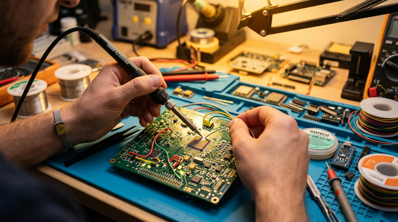
- Start with a requirements matrix that maps every functional requirement to a specific hardware peripheral and software module—before you touch a schematic.
- Select your MCU/MPU family based on peripheral fit, long-term availability (10+ year lifecycle), and toolchain maturity—not just clock speed or price.
- Build your BSP (Board Support Package) and hardware abstraction layer early; this is the layer that determines whether your firmware survives a chip swap in three years.
- Validate power, thermal, and EMC constraints on a prototype board before committing to a production layout—rework on a 10-layer HDI stackup costs $15K–$40K per spin.
- Integrate CI/CD for firmware from day one using real hardware-in-the-loop (HIL) testing, not just host-compiled unit tests.
Designing an embedded system from scratch means making a series of tightly coupled hardware and software decisions—processor selection, memory architecture, peripheral allocation, power domain design, BSP bring-up, RTOS selection, and firmware architecture—in the correct order, with the right tradeoffs documented at every gate. There’s no single “right” architecture. But there is a repeatable engineering process that gets you from a requirements document to a production-ready, certifiable system without burning three board spins and six months of schedule. This guide walks through that process, step by step, with real part numbers, real toolchains, and the decisions that actually matter.
What Hardware Platform Should You Choose for a New Embedded Design?
This is the decision that constrains everything downstream. Get it wrong and you’re stuck with a processor that can’t meet your real-time deadlines, a memory bus that bottlenecks your data pipeline, or a part that goes EOL 18 months after your product ships. Get it right and the firmware architecture nearly writes itself.
How Do You Map Requirements to Silicon?
Start with a peripheral requirements matrix. Every sensor interface, communication bus, actuator driver, and external memory channel needs a row. Columns are candidate processors. Fill in whether the peripheral is native, requires an external IC, or is unsupported. This matrix is the single most valuable artifact in early-stage embedded design.
For a mid-complexity industrial IoT gateway, you might compare the NXP i.MX 93 (dual Cortex-A55, Cortex-M33 real-time domain, EtherCAT-capable), the STMicroelectronics STM32MP257 (dual Cortex-A35, Cortex-M33, integrated TSN Ethernet), and the TI AM6254 (quad Cortex-A53, Cortex-M4F, PRU-ICSS subsystem for custom industrial protocols). Each has a different answer to “can I run a Linux application stack and still hit 10 µs control loop deadlines on the real-time core?”
Key insight: The real-time core’s interrupt latency matters more than the application processor’s clock speed in 90% of embedded control designs. Profile worst-case ISR latency on eval hardware before committing.
For deeply embedded, battery-powered sensor nodes, the decision space shifts to microcontrollers. The STM32U5 series (Cortex-M33, TrustZone, sub-µA stop modes) competes with the Nordic nRF5340 (dual-core, integrated BLE 5.4) and the Renesas RA6M5 (Cortex-M33, USB HS, CAN FD). Per recent EE Times survey data, roughly 68% of new IoT sensor designs target sub-10 mW average power—which immediately disqualifies anything without aggressive low-power modes and peripheral gating.
When Does an FPGA or SoC-FPGA Make Sense?
When your data path requires deterministic, parallel processing that no MCU or DSP can hit in software—think high-speed ADC capture, custom protocol engines, or sensor-fusion pipelines that need to process data within a fixed number of clock cycles. The Xilinx Zynq UltraScale+ ZCU208 (XCZU48DR-2FSVG1517E) is the standard eval platform for RF-class designs where you need both programmable logic and embedded ARM Cortex-A53/R5F cores. Teams at IAI and Rafael typically pair Zynq UltraScale+ devices with AMD Vitis (formerly Xilinx Vitis) for SDR and radar signal processing workloads.
For lower-cost, lower-gate-count applications, the Intel (Altera) Cyclone V SoC or the Lattice CertusPro-NX offer a more reasonable BOM. Don’t reach for an FPGA because it’s technically interesting—reach for it because your timing analysis proves the MCU can’t close the loop.
How Do You Architect Firmware That Survives Production?
Production firmware isn’t a demo that happens to work. It handles every error path, recovers from power glitches, updates itself in the field without bricking, and passes EMC testing on the first shot. The architecture decisions you make in the first two weeks determine whether that’s achievable or whether you’re firefighting errata for six months.
What RTOS Should You Use—and When Is Bare-Metal Enough?
If your system has more than one time-critical task with different deadlines, you need an RTOS. The question is which one. For commercial and industrial work, FreeRTOS (now maintained by AWS under the MIT license) is the default—deployed on an estimated 40%+ of 32-bit MCUs shipped worldwide per recent IoT Analytics data. For safety-critical or defense applications, you’re looking at SAFERTOS (the IEC 61508 / DO-178C certifiable derivative of FreeRTOS), Zephyr RTOS (Linux Foundation–backed, growing rapidly in automotive and industrial), or a POSIX-compliant RTOS like QNX Neutrino 7.1 or VxWorks 23.09.
Defense primes such as Elbit Systems and L3Harris favor PREEMPT_RT Linux for sub-millisecond soft-real-time control loops on Cortex-A class processors, reserving the Cortex-R or Cortex-M real-time islands for hard-real-time tasks. This asymmetric multiprocessing (AMP) pattern—Linux on the application core, RTOS on the real-time core—is the dominant architecture for anything with both a UI/networking stack and deterministic control.
Bare-metal (superloop) is still the right call for single-function sensor nodes where every microamp counts and the task model is simple enough to express as a state machine driven by timer interrupts. If you find yourself implementing a hand-rolled task scheduler in a superloop, stop—you’ve just reinvented a bad RTOS.
How Do You Structure the Hardware Abstraction Layer?
The HAL is the layer that lets you swap an STM32H7 for an STM32U5—or even an NXP i.MX RT1170—without rewriting application logic. It’s also the layer most teams get wrong, either by making it too thin (a macro wrapper around register writes) or too thick (a full POSIX shim on a Cortex-M0).
A practical HAL for a Cortex-M target has four layers:
- Register access layer — CMSIS-compatible header files, auto-generated from SVD (System View Description) files. Use the vendor’s headers; don’t hand-roll them.
- Peripheral driver layer — Thin drivers for UART, SPI, I2C, GPIO, ADC, timers. Each driver exposes init, read, write, deinit, and an ISR callback registration API. No blocking calls—everything is interrupt-driven or DMA-driven.
- Board support layer — Pin mux, clock tree configuration, power domain sequencing. This is the only layer that changes when you rev the PCB.
- Application interface layer — Abstract “sensor,” “actuator,” “comms channel” interfaces that the application code calls. This is the portability boundary.
Common mistake: Using STM32CubeMX-generated HAL code as your production HAL. It’s fine for prototyping, but the auto-generated code is bloated, hard to unit-test, and couples your application logic to ST’s code generation tool. Extract what you need into your own driver layer and own it.
Here’s a minimal HAL UART initialization for an STM32H753 (Cortex-M7, 480 MHz) using direct register access under FreeRTOS, showing the pattern:
/* hal_uart.c — UART3 on STM32H753, DMA-backed TX, interrupt-driven RX */
#include "stm32h7xx.h"
#include "FreeRTOS.h"
#include "semphr.h"

static SemaphoreHandle_t uart3_tx_sem;
static volatile uint8_t  rx_ring[256];
static volatile uint16_t rx_head = 0, rx_tail = 0;

void hal_uart3_init(uint32_t baudrate) {
    /* Enable clocks: USART3 on APB1, GPIOD for PD8/PD9 */
    RCC->APB1LENR |= RCC_APB1LENR_USART3EN;
    RCC->AHB4ENR  |= RCC_AHB4ENR_GPIODEN;

    /* PD8 = TX (AF7), PD9 = RX (AF7) */
    GPIOD->MODER   &= ~(0xF << 16);
    GPIOD->MODER   |=  (0xA << 16);   /* alternate function */
    GPIOD->AFR[1]  &= ~(0xFF << 0);
    GPIOD->AFR[1]  |=  (0x77 << 0);   /* AF7 for PD8, PD9 */

    /* Baudrate: assuming 120 MHz APB1 clock */
    USART3->BRR = 120000000UL / baudrate;
    USART3->CR1 = USART_CR1_TE | USART_CR1_RE | USART_CR1_RXNEIE;
    USART3->CR1 |= USART_CR1_UE;

    NVIC_SetPriority(USART3_IRQn, configLIBRARY_MAX_SYSCALL_INTERRUPT_PRIORITY + 1);
    NVIC_EnableIRQ(USART3_IRQn);

    uart3_tx_sem = xSemaphoreCreateBinary();
    xSemaphoreGive(uart3_tx_sem);
}

void USART3_IRQHandler(void) {
    if (USART3->ISR & USART_ISR_RXNE) {
        rx_ring[rx_head++ & 0xFF] = (uint8_t)USART3->RDR;
    }
}
That’s roughly 40 lines. It initializes the peripheral, sets up interrupt-driven receive into a ring buffer, and provides a FreeRTOS semaphore for TX arbitration. Production code adds error flag handling (ORE, FE, NE), DMA for TX, and a proper ring buffer abstraction—but the structure is the same.
How Do You Set Up CI/CD for Embedded Firmware?
Per recent JetBrains developer survey data, only about 35% of embedded teams run automated firmware builds on every commit. The rest build on developer machines, hope the toolchain versions match, and discover integration bugs during system test. That’s how schedule slips happen.
What Does a Minimal Embedded CI Pipeline Look Like?
At minimum, you need: (1) a reproducible build environment (Docker container with your cross-compiler), (2) automated build on every push, (3) static analysis (MISRA C or CERT C), and (4) host-compiled unit tests. Hardware-in-the-loop testing is the next tier.
Here’s a real GitLab CI configuration for an STM32H7 project using arm-none-eabi-gcc 13.2 and Cppcheck:
# .gitlab-ci.yml — Embedded firmware CI for STM32H7
image: registry.example.com/embedded/stm32-toolchain:13.2

stages:
  - build
  - analyze
  - test

variables:
  GCC_ARM: /opt/gcc-arm-none-eabi-13.2/bin
  BUILD_DIR: build/release

build_firmware:
  stage: build
  script:
    - export PATH=$GCC_ARM:$PATH
    - mkdir -p $BUILD_DIR
    - cmake -B $BUILD_DIR -DCMAKE_TOOLCHAIN_FILE=cmake/stm32h753.cmake -DCMAKE_BUILD_TYPE=Release
    - cmake --build $BUILD_DIR -j$(nproc)
    - arm-none-eabi-size $BUILD_DIR/firmware.elf
  artifacts:
    paths:
      - build/release/firmware.elf
      - build/release/firmware.bin

static_analysis:
  stage: analyze
  script:
    - cppcheck --enable=all --std=c11 --suppress=missingIncludeSystem
        --inline-suppr --error-exitcode=1
        -I src/hal -I src/app -I src/drivers
        src/
  allow_failure: false

unit_tests:
  stage: test
  image: gcc:13
  script:
    - mkdir -p build/test
    - cmake -B build/test -DTARGET=host_test
    - cmake --build build/test -j$(nproc)
    - cd build/test && ctest --output-on-failure
This pipeline catches three classes of bugs that typically survive to system integration: build reproducibility issues (wrong toolchain version), static analysis violations (null pointer dereferences, buffer overflows, MISRA rule violations), and logic bugs in platform-independent code (protocol parsers, state machines, math functions). It runs in under two minutes on a standard GitLab runner.
For hardware-in-the-loop, we’ve deployed setups where a GitLab runner has physical access to a target board (STM32H753 Nucleo-144 or custom hardware) via a Segger J-Link and runs integration tests using PyOCD for flashing and a Python test harness over UART. It adds five minutes to the pipeline but catches DMA configuration errors, clock tree misconfiguration, and peripheral initialization ordering bugs that host-compiled tests can never find.
How Do You Handle Power, Thermal, and EMC in the Hardware Design?
What Are the Critical Power Domain Decisions?
Every modern embedded processor has multiple power domains—core, I/O, analog, PLL, real-time. The sequencing of these domains at startup and the ability to selectively shut them down in sleep modes determines your system’s power profile. On the NXP i.MX 95 (up to six Cortex-A55 cores, Cortex-M33, Cortex-M7, and an eIQ Neutron NPU), there are 14 independently controllable power domains. Mis-sequencing them doesn’t just waste power